Nano 'pin art': NIST arrays are step toward mass production of nanowires
02 Aug 2010
Researchers at the National Institute of Standards and Technology (NIST) have cultivated many thousands of nanocrystals in what looks like a pinscreen or "pin art" on silicon, a step toward reliable mass production of semiconductor nanowires for millionths-of-a-meter-scale devices such as sensors and lasers.
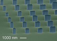 |
| Colorized micrograph of semiconductor nanowires grown at NIST in a precisely controlled array of sizes and locations. Credit: K. Bertness/NIST |
Colorized micrograph of semiconductor nanowires grown at NIST in a precisely controlled array of sizes and locations.
NIST researchers grow nanowires made of semiconductors - gallium nitride alloys - by depositing atoms layer-by-layer on a silicon crystal under high vacuum.
NIST has the unusual capability to produce these nanowires without using metal catalysts, thereby enhancing luminescence and reducing defects. NIST nanowires also have excellent mechanical quality factors.
The latest experiments, described in Advanced Functional Materials,* maintained the purity and defect-free crystal structure of NIST nanowires while controlling diameter and placement better than has been reported by other groups for catalyst-based nanowires.
Precise control of diameter and placement is essential before nanowires can be widely used. (* K. A. Bertness, A. W. Sanders, D. M. Rourke, T. E. Harvey, A. Roshko, J.B. Schlager and N. A. Sanford. Controlled nucleation of GaN nanowires grown with molecular beam epitaxy. Advanced Functional Materials. Published online: July 13, 2010. DOI: 10.1002/adfm.201000381)