The future of chip manufacturing
By Larry Hardesty, MIT News Office | 01 Jul 2011
For 50 years, the transistors on computer chips have been getting smaller, and for 50 years, manufacturers have used the same technique - photolithography - to make their chips. But the very wavelength of visible light limits the size of the transistors that photolithography can produce. If chipmakers are to keep shrinking chip features, they'll probably need to turn to other manufacturing methods.
 |
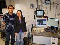
| Research Laboratory of Electronics graduate students Vitor Manfrinato and Lin Lee Cheong, with the electron-beam lithography system they used in their experiments. Photo: Melanie Gonick |
Researchers have long used a technique called electron-beam (or e-beam) lithography to make prototype chips, but standard e-beam lithography is much slower than photolithography.
Increasing its speed generally comes at the expense of resolution: previously, the smallest chip features that high-speed e-beams could resolve were 25 nanometers across, barely better than the experimental 32-nanometer photolithography systems that several manufacturers have demonstrated. In a forthcoming issue of the journal Microelectronic Engineering, however, researchers at MIT's Research Laboratory of Electronics (RLE) present a way to get the resolution of high-speed e-beam lithography down to just nine nanometers.
Combined with other emerging technologies, it could point the way toward making e-beam lithography practical as a mass-production technique.
The most intuitive way for manufacturers to keep shrinking chip features is to switch to shorter wavelengths of light - what's known in the industry as extreme ultraviolet. But that's easier said than done.
''Because the wavelength is so small, the optics [are] all different,'' says Vitor Manfrinato, an RLE graduate student and first author on the new paper. ''So the systems are much more complicated … [and] the light source is very inefficient.''


