New technique could harvest more of the Sun's energy
28 Nov 2014
As solar panels become less expensive and capable of generating more power, solar energy is becoming a more commercially viable alternative source of electricity.
 | |
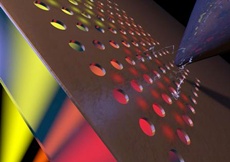
| An ultra-sensitive needle measures the voltage that is generated while the nanospheres are illuminated /Credit: AMOLF/Tremani - Figure: Artist impression of the plasmo-electric effec |
However, the photovoltaic cells now used to turn sunlight into electricity can only absorb and use a small fraction of that light, and that means a significant amount of solar energy goes untapped.
A new technology created by researchers from California Institute of Technology (Caltech), and described in a paper published online in the 30 October issue of Science Express, represents a first step toward harnessing that lost energy.
Sunlight is composed of many wavelengths of light. In a traditional solar panel, silicon atoms are struck by sunlight and the atoms' outermost electrons absorb energy from some of these wavelengths of sunlight, causing the electrons to get excited.
Once the excited electrons absorb enough energy to jump free from the silicon atoms, they can flow independently through the material to produce electricity. This is called the photovoltaic effect - a phenomenon that takes place in a solar panel's photovoltaic cells.
Although silicon-based photovoltaic cells can absorb light wavelengths that fall in the visible spectrum - light that is visible to the human eye - longer wavelengths such as infrared light pass through the silicon. These wavelengths of light pass right through the silicon and never get converted to electricity - and in the case of infrared, they are normally lost as unwanted heat.
"The silicon absorbs only a certain fraction of the spectrum, and it's transparent to the rest," says Harry A. Atwater, the Howard Hughes Professor of Applied Physics and Materials Science; director, Resnick Sustainability Institute, who led the study.
"If I put a photovoltaic module on my roof, the silicon absorbs that portion of the spectrum, and some of that light gets converted into power. But the rest of it ends up just heating up my roof."
Now, Atwater and his colleagues have found a way to absorb and make use of these infrared waves with a structure composed not of silicon, but entirely of metal.
The new technique they've developed is based on a phenomenon observed in metallic structures known as plasmon resonance. Plasmons are coordinated waves, or ripples, of electrons that exist on the surfaces of metals at the point where the metal meets the air.
While the plasmon resonances of metals are predetermined in nature, Atwater and his colleagues found that those resonances are capable of being tuned to other wavelengths when the metals are made into tiny nanostructures in the lab.
"Normally in a metal like silver or copper or gold, the density of electrons in that metal is fixed; it's just a property of the material," Atwater says. "But in the lab, I can add electrons to the atoms of metal nanostructures and charge them up. And when I do that, the resonance frequency will change."
"We've demonstrated that these resonantly excited metal surfaces can produce a potential"-an effect very similar to rubbing a glass rod with a piece of fur: you deposit electrons on the glass rod. "You charge it up, or build up an electrostatic charge that can be discharged as a mild shock," he says. "So similarly, exciting these metal nanostructures near their resonance charges up those metal structures, producing an electrostatic potential that you can measure."
This electrostatic potential is a first step in the creation of electricity, Atwater says. "If we can develop a way to produce a steady-state current, this could potentially be a power source. He envisions a solar cell using the plasmoelectric effect someday being used in tandem with photovoltaic cells to harness both visible and infrared light for the creation of electricity.
Although such solar cells are still on the horizon, the new technique could even now be incorporated into new types of sensors that detect light based on the electrostatic potential.
"Like all such inventions or discoveries, the path of this technology is unpredictable," Atwater says. "But any time you can demonstrate a new effect to create a sensor for light, that finding has almost always yielded some kind of new product."
This work was published in a paper titled, Plasmoelectric Potentials in Metal Nanostructures. Other coauthors include first author Matthew T. Sheldon, a former postdoctoral scholar at Caltech; Ana M. Brown, an applied physics graduate student at Caltech; and Jorik van de Groep and Albert Polman from the FOM Institute AMOLF in Amsterdam. The study was funded by the Department of Energy, the Netherlands Organization for Scientific Research, and an NSF Graduate Research Fellowship.


