Important step toward computing with light
By By David L. Chandler, MIT News Office | 23 Nov 2011
There has been enormous progress in recent years toward the development of photonic chips - devices that use light beams instead of electrons to carry out their computational tasks. Now, researchers at MIT have filled in a crucial piece of the puzzle that could enable the creation of photonic chips on the standard silicon material that forms the basis for most of today's electronics.
 In many of today's communication systems, data travels via light beams transmitted through optical fibres. Once the optical signal arrives at its destination, it is converted to electronic form, processed through electronic circuits and then converted back to light using a laser. The new device could eliminate those extra electronic-conversion steps, allowing the light signal to be processed directly.
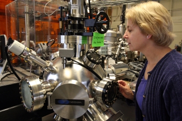
The new component is a ''diode for light,'' says Caroline Ross, the Toyota Professor of materials science and engineering at MIT, who is co-author of a paper reporting the new device that was published online 13 November in the journal Nature Photonics.
It is analogous to an electronic diode, a device that allows an electric current to flow in one direction but blocks it from going the other way; in this case, it creates a one-way street for light, rather than electricity.
This is essential, Ross explains, because without such a device stray reflections could destabilise the lasers used to produce the optical signals and reduce the efficiency of the transmission. Currently, a discrete device called an isolator is used to perform this function, but the new system would allow this function to be part of the same chip that carries out other signal-processing tasks.
To develop the device, the researchers had to find a material that is both transparent and magnetic - two characteristics that rarely occur together. They ended up using a form of a material called garnet, which is normally difficult to grow on the silicon wafers used for microchips. Garnet is desirable because it inherently transmits light differently in one direction than in another: It has a different index of refraction - the bending of light as it enters the material - depending on the direction of the beam.
The researchers were able to deposit a thin film of garnet to cover one half of a loop connected to a light-transmitting channel on the chip. The result was that light traveling through the chip in one direction passes freely, while a beam going the other way gets diverted into the loop.
The whole system could be made using standard microchip manufacturing machinery, Ross says.
''It simplifies making an all-optical chip,'' she says. The design of the circuit can be produced ''just like an integrated-circuit person can design a whole microprocessor. Now, you can do an integrated optical circuit.''
That could make it much easier to commercialise than a system based on different materials, Ross says. ''A silicon platform is what you want to use,'' she says, because ''there's a huge infrastructure for silicon processing. Everyone knows how to process silicon. That means they can set about developing the chip without having to worry about new fabrication techniques.''
This technology could greatly boost the speed of data-transmission systems, for two reasons: First, light travels much faster than electrons. Second, while wires can only carry a single electronic data stream, optical computing enables multiple beams of light, carrying separate streams of data, to pass through a single optical fibre or circuit without interference. ''This may be the next generation in terms of speed'' for communications systems, Ross says.
Ross' colleagues in the research included Lionel Kimerling, the Thomas Lord Professor of Materials Science and Engineering, and former students Lei Bi '11 and Juejun Hu PhD '09. The work was funded by the National Science Foundation and an Intel fellowship for Bi.
''This is a big advance in optical communications,'' says Bethanie Stadler, a professor of electrical and computer engineering at the University of Minnesota, who was not involved in this research. The work is ''significant,'' she says, ''as the first device with garnet integrated onto [silicon] devices.''